VLSI Digital System Algorithms and Architectures
What Happens Below the Logic
1/25/20268 min read
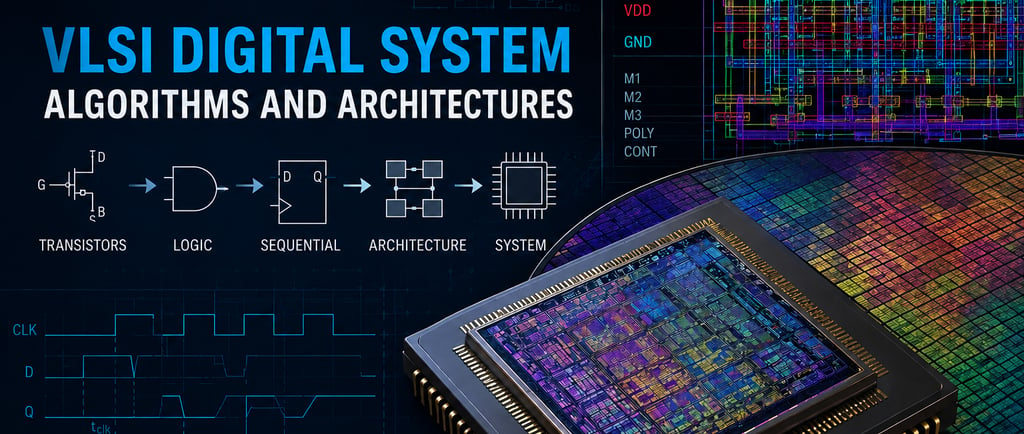
I'd never taken a VLSI (comically short for Very Large Scale Integration) course before this. In undergrad, my exposure to chip design ended at logic gates and maybe some basic timing analysis. I knew what a NAND gate was, I could draw a state machine, but the actual physics of how that became transistors on silicon was a black box. So when I walked into ECE 260A in fall 2018, I was starting from scratch while most of my classmates were already familiar with tapeouts. The first few weeks were disorienting. People casually referenced N-wells and layout density and polysilicon contacts, and I was trying to figure out what those terms even meant.
The course description promised custom and semicustom VLSI design from both circuit and system perspectives: MOS transistor theory, circuit characterization, performance estimation, CMOS logic design, and hands-on work with CAD tools. What that actually meant was learning to think about digital circuits as physical objects with real constraints, not just as Boolean abstractions.
What Were the Core Ideas?
Looking back six years later, a few concepts have stuck while most of the specific equations and circuit topologies have faded.
The first was understanding that the abstraction ladder goes both directions. We started at MOS transistor physics: threshold voltages, channel length modulation, body effect. We worked up through logic gates and timing analysis to full architectures. But you couldn't just design at the architectural level and assume the transistor-level details would work themselves out. An architectural choice like using a ripple-carry adder versus a carry-lookahead adder had direct consequences for transistor sizing, layout density, and power consumption. The layers weren't independent. Decisions at one level propagated up and down the stack.
The second was that signal propagation is physics, not just logic. Coming from a digital design background, I'd always been able to think of signals as clean 1s and 0s that switched instantaneously. This course forced me to confront the messier reality: every transition takes time, consumes energy, and couples capacitively to neighboring wires. We spent a lot of time tracing signal paths through architectures while accounting for RC delays, clock skew, setup and hold violations. Logic gates aren't just Boolean functions. They're analog circuits that happen to spend most of their time near the supply rails.
The third idea was that design is constraint optimization. Every decision involved trading off speed, power, and area, and you could rarely improve one without giving up something in the others. Want a faster circuit? Add more transistors, which costs area. Or increase drive strength, which costs power. Cadence made this concrete. You'd simulate a design, see it was too slow, resize some transistors, watch power consumption spike, iterate again. The course was as much about learning to navigate those tradeoffs as it was about learning the tools.
The fourth, which I didn't fully appreciate at the time, was that tools are essential but imperfect. We used the Cadence suite for everything: schematic capture, layout in Virtuoso, circuit simulation, DRC and LVS for verification. Learning the tools felt like learning a language with arcane syntax and mysterious failure modes. Every step required configuring dozens of settings: process corners, temperature ranges, supply voltage variations, parasitic extraction modes. You had to know which models to use, which checks to enable, what tolerance to accept for different violations. But the real lesson was understanding what the tools were doing under the hood. Parasitic extraction made assumptions about coupling capacitance. Corner case analysis relied on models that might not capture every edge case. You couldn't just trust the tools blindly. You needed to know when to question the results.
What Has Changed Since 2018-2020?
Process technology has continued to advance. We designed for what I think was a 30nm process in the labs. Leading-edge chips are now at 3nm and heading toward 2nm, but the bigger shift has been in priorities. When I took the course, power was one of several concerns. Now it's often the dominant constraint, especially with edge AI and the end of Dennard scaling. Chiplets and heterogeneous integration have become major trends, changing what VLSI design even means. It's less about optimizing a single monolithic die and more about integrating multiple specialized dies.
The open-source ecosystem has changed dramatically. In June 2020, around the time I was finishing the program, Google and SkyWater Technology released the first open-source Process Design Kit for a commercial 130nm process. When I was taking ECE 260A, the idea of downloading a complete PDK from GitHub and designing manufacturable chips without NDAs or expensive licenses seemed impossible. Now there are complete open-source flows from RTL to GDSII using tools like OpenROAD, Magic, and Yosys. Programs like Tiny Tapeout let you go from idea to fabricated chip for ~$100. The barrier to entry has dropped in ways that would have seemed absurd in 2018.
AI has started appearing in EDA tools, though I'm not sure yet how much of it is substance versus hype. Machine learning is being used for placement optimization, timing closure prediction, and design space exploration. The tools haven't replaced human designers, but they're handling more of the tedious optimization work that we did manually.
Cloud-based EDA is another shift. When I took the course, we had a limited number of compute servers that we had to reserve time on. Now physical design can scale across thousands of virtual CPUs in the cloud, letting teams run parallel simulations and iterate faster.
What hasn't changed: the physics. RC delays, parasitic capacitance, timing closure. These are still the fundamental challenges, just manifested differently at smaller nodes. The core concepts of CMOS logic design are still foundational. And the commercial EDA market is still dominated by the same players: Cadence, Synopsys, and Siemens EDA.
What Actually Mattered?
The mental models of signal propagation turned out to be more useful than I expected. I haven't done IC design professionally, but understanding how signals actually behave has been valuable for debugging high-speed digital systems and understanding PCB design constraints. Finite rise times, reflections, crosstalk: these all matter when you're working at speeds where the physical layer can't be ignored. It's one thing to know intellectually that signals aren't instantaneous. It's another to have worked through the math of how RC delays accumulate and where transmission line effects start to matter.
The constraint optimization mindset transferred well beyond VLSI. The speed-power-area tradeoff shows up everywhere, just with different parameters. Project Management: scope-cost-time. RF Design: bandwidth-power-linearity. Learning to think in constraint spaces and recognize when you're trading one thing for another has been one of the more broadly applicable skills from this course.
The course also forced me to get comfortable reading technical documentation. We spent a lot of time digging through process design kits, understanding timing parameters, figuring out what was guaranteed versus what was typical. Being able to parse dense technical specs and extract what actually matters is a skill I've used constantly.
What mattered less: the specific Cadence workflows. Tools evolve, interfaces change, and unless you're doing IC design full-time, the particular menu navigation and command syntax fade quickly. What stuck was the conceptual understanding of what each step was checking for. DRC verifies that the layout meets manufacturing constraints. LVS checks that the layout matches the schematic. Parasitic extraction models the non-ideal behavior of interconnects. Knowing what the tools do matters more than knowing exactly how to drive them.
Hand calculations for transistor sizing also hardly matter. In practice, simulation tools handle the grunt work. The value was in understanding the equations well enough to sanity-check results and recognize when a simulation was giving nonsense, but you won't find anyone crunching these numbers by hand in a commercial setting.
I've never directly used the MOS transistor physics I learned at the equation level. I've never used the drain current equation in a commercial role, and I've never needed to calculate subthreshold swing or channel length modulation in my work. But having that mental model of how transistors actually work (the role of the gate, the channel, the threshold voltage) has been useful context for understanding device behavior and limitations in application settings.
What Would I Prioritize If I Were Taking It Today?
If I were taking this course now, knowing what I know about where my career went, I'd spend more time on power analysis and optimization. Power has become central to modern chip design in ways that weren't as obvious in 2018. Understanding dynamic versus static power, power gating techniques, and voltage scaling tradeoffs would be worth digging into more deeply. We covered them, but they felt like one topic among many. Now they're often the primary constraint.
I'd also go deeper on timing closure and clock domain crossing. These were covered, but I'd prioritize them more. A lot of real-world hardware problems come down to timing: setup and hold violations, clock skew, metastability. Understanding the practical techniques for managing timing in complex designs would have made debugging hardware systems easier later.
The interface between digital and analog is another area I'd explore more. We touched on this with CMOS circuits and I/O drivers, but most interesting problems live at these boundaries. Mixed-signal design, how digital signals interact with the analog world, what happens at power rails and ground planes. This is where a lot of subtle bugs hide.
On the other hand, I'd spend less time on low-level layout techniques for the specific process we used in labs. Learning layout fundamentals is important, but optimizing layouts for a 30nm process has limited practical value now. I'd focus more on understanding modern design flows and how automation tools work.
We covered a lot of different logic families in the course: pass-transistor logic, domino logic, various flavors of dynamic logic. Interesting from an academic perspective, but for most purposes, understanding standard CMOS and maybe one alternative would suffice. I'd skim the rest unless I ended up working specifically in low-power design where these techniques matter.
If I could add topics, I'd want more on design for manufacturability and reliability. Process variation, aging effects, soft errors. These weren't emphasized much but they're critical for chips that need to work reliably over years in the field. We focused on getting the design functionally correct, but production-level chip design has to account for all the ways things can degrade or vary from the ideal case.
I'd also be curious to learn the same concepts through open-source tools. Working with Magic, ngspice, and open PDKs alongside Cadence would make the knowledge more portable and accessible. The commercial tools are more polished, but understanding how to work with open-source alternatives would be valuable now that those ecosystems have matured.
Six years out, what I remember most from this course isn't the specific circuit topologies or the exact steps for running DRC. It's the shift in how I thought about digital systems. I came in with an understanding of digital circuits as abstractions. By the end, I had a much better grasp of the physical implementation underneath it. Signals take time to propagate. Wires have capacitance. Transistors leak current. The abstractions only work if you respect what's happening at the layers below.
This course was hard, and not just on its own terms. I was taking three courses that first quarter while working full time, and I was still figuring out how to be a student again after a few years away from coursework. The combination meant I was always behind, always catching up on weekends, and rarely felt like I had solid footing. But it gave me an early appreciation for the complexity of what I'd signed up for. This was going to be two years of material that moved fast and assumed you could keep up. ECE 260A made that clear immediately.