Solid State Electronics
Six layers of abstraction below my day job
2/1/202610 min read
I'll be honest up front: I did not understand most of this course. ECE 230A was graduate-level semiconductor physics, and while I'd taken a materials science class as part of my undergrad EE coursework, that preparation turned out to be thinner than I'd assumed. I spent a lot of the quarter just trying to understand the basic terminology being used, let alone applying it at the level the course expected. People around me were working through problem sets with a fluency I couldn't match. I was still trying to figure out what a density of states was while my classmates were using it to calculate carrier concentrations.
The course description said it would provide "a general background in solid state electronic materials and devices" with emphasis on "fundamental and current issues of semiconductor physics." In practice, that meant starting from crystal structure and quantum mechanics and building up through carrier transport, doping, junction behavior, and MOS device physics. The textbook was dense and the lectures moved fast. I was frequently lost during class, not just struggling with the problem sets afterward but losing the thread of the lecture itself. The material built on itself, so falling behind on one concept meant the next three were harder to follow.
I took this alongside ECE 260A and digital image processing, which meant my first quarter was three courses that each demanded a different kind of thinking. VLSI was about design tradeoffs and tool flows. Image processing was applied linear algebra. Solid state electronics was physics, the kind where you have to hold multiple abstract concepts in your head simultaneously and reason about what happens when they interact. It was the most conceptually demanding of the three, and the one where I felt the least confident throughout. Looking back six years later, I'd say I came away with an understanding of the vocabulary and what the concepts were trying to accomplish, even if I never felt like I truly had a grasp on the material itself.
What Were the Core Ideas?
I want to be careful here, because "core ideas that stayed with me" implies a level of retention I'm not sure I earned. What stayed with me is more like an awareness of what the ideas were and why they mattered, rather than the ability to work with them in any rigorous way.
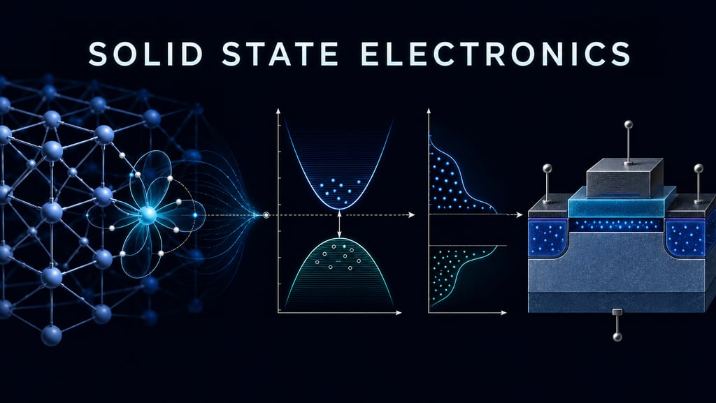
One thing I do remember clearly is being struck by the audacity of the insights in each topic. We were reasoning about individual dopant atoms in a crystal lattice, electrons occupying quantum energy states, electric fields across regions measured in nanometers. Each of those topics represents someone, at some point, figuring out how to characterize something that can't be directly observed and building a quantitative framework around it. And then the entire field of semiconductor engineering stacks those frameworks on top of each other, layer after layer, until you get something as useful as a transistor. I kept thinking about how improbable that chain of understanding was, that each link required its own set of insights and experiments, and that the whole thing only works because each level turned out to be well-enough behaved to abstract over.
The first was that semiconductor behavior is fundamentally statistical. You aren't tracking individual electrons. You're reasoning about populations of carriers described by probability distributions and energy-dependent density of states. The Fermi-Dirac distribution, the Boltzmann approximation, the concept of a Fermi level that shifts with doping and temperature: these form the vocabulary for describing what's happening inside a semiconductor. I remember struggling with this because my intuition wanted to think about electrons as discrete things moving through a lattice. The statistical perspective felt abstract and disconnected from anything I could visualize. I understood that this was a more honest description of what's happening at scale, but I never developed the kind of working fluency where I could pick up a problem and know which tools to apply.
The second was the energy band model and how it explains the difference between metals, semiconductors, and insulators. The band structure is the foundation for everything else in the course: why silicon conducts under certain conditions, what doping actually does at the atomic level, how light interacts with semiconductor materials, why some materials have direct bandgaps and others don't. We spent a lot of time drawing band diagrams, first for bulk semiconductors, then for junctions and interfaces. I understood the goal of band diagrams as a reasoning tool, and I could follow the logic when someone walked me through one. But generating them from scratch for a new situation was something I could only do for the simplest cases.
The third was carrier transport: drift and diffusion. Drift is the movement of carriers under an electric field. Diffusion is movement driven by concentration gradients. Both happen simultaneously in most semiconductor devices, and the interplay between them determines how current flows. The continuity equation, which combines generation, recombination, drift, and diffusion into one framework, was probably the most important equation in the course. I remember recognizing its importance, that it tied everything together, without being able to wield it confidently on exams.
The fourth was pn junction behavior. This was where the course transitioned from physics to devices, and where things started to feel slightly more tangible. A pn junction is conceptually approachable: put p-type and n-type material together and a depletion region forms. But the detailed analysis of what happens under forward and reverse bias, how the built-in potential arises, how minority carrier injection works: all of this requires the statistical and transport frameworks from earlier in the course. If those foundations were shaky, and mine were, the junction analysis never quite solidified either. I understood the picture of what was happening. I could describe it in words. The math was another story.
The fifth was MOS device physics. We covered the MOS capacitor in detail: accumulation, depletion, inversion, threshold voltage. This connected directly to the MOSFET operation I was learning about in ECE 260A, but from the physics side rather than the circuit side. Of everything in the course, this section felt the most relevant to my work, because I could connect it to things I actually designed with. Understanding what was happening at the oxide-semiconductor interface, even at a high level, gave me context that the circuit-level treatment alone wouldn't have provided.
What Has Changed Since 2018-2020?
The core physics hasn't changed. Semiconductor band theory, carrier transport equations, and junction electrostatics are the same as they were when Shockley and Bardeen were working on them. What has changed is which device structures matter and which material systems are getting serious attention.
The biggest shift in device architecture is the transition from FinFETs to gate-all-around nanosheet transistors. When I took this course in 2018, FinFETs were the dominant advanced transistor structure. We studied planar MOSFETs in detail, and FinFETs were discussed as the modern evolution. Now, the industry is moving to nanosheets where the gate wraps around the channel on all four sides rather than three. Samsung began producing GAA devices at its 3nm node, and TSMC is ramping GAA production at 2nm in 2025. Intel's version, called RibbonFET, is part of its 20A and 18A process nodes. The physics we studied, channel control, short-channel effects, threshold voltage engineering, are exactly the concepts that explain why this transition is happening. As channels get shorter, you need more gate control to suppress leakage, and wrapping the gate around the entire channel is the logical endpoint of that trend.
Looking further ahead, the semiconductor industry is already developing complementary FET (CFET) structures, where NFET and PFET transistors are stacked vertically on top of each other rather than placed side by side. At IEDM 2025, TSMC demonstrated the first fully functional CFET ring oscillator with gate pitches below 48nm. Imec's roadmap places CFET production around 2031. This is where the device physics from a course like ECE 230A becomes directly relevant: understanding how to engineer threshold voltages, manage self-heating, and control carrier behavior in increasingly constrained geometries all traces back to the fundamentals.
Another major development is backside power delivery, where the power distribution network is moved from the front of the wafer to the back. Intel demonstrated this with its PowerVia technology, and TSMC plans to integrate its Super PowerRail architecture at the A16 node. Routing power through thinned silicon substrates using nano-scale through-silicon vias requires understanding carrier behavior, contact resistance, and thermal transport at scales where bulk assumptions start to break down.
Wide bandgap semiconductors have gone from research curiosity to commercial reality. Silicon carbide power devices are now standard in electric vehicle inverters, and GaN is widely used in fast chargers, data center power supplies, and RF amplifiers. The market for SiC and GaN power devices was valued at around $1.4 billion in 2024 and is growing at roughly 20% annually. When I took ECE 230A, we focused almost entirely on silicon. The band theory and carrier transport physics apply to any semiconductor material, but we didn't spend much time thinking about what changes when you move to a material with a 3.3 eV bandgap instead of 1.1 eV. That shift in material emphasis is one of the more significant changes in how this subject would be taught today.
What hasn't changed: the MOSFET is still the most important electronic device ever made, and the physics that governs it is the same physics we studied. The device structures have become more complex, but the underlying principles remain the foundation that everything else is built on.
What Actually Mattered?
This is the section where I have to be most honest, because the answer is: less than I'd like. I haven't solved a drift-diffusion equation since the final exam, and I'd have to look up the form of the Fermi-Dirac integral if someone asked me to use it. The specific problem-solving techniques are gone. What remains is more like a vocabulary and a set of directional intuitions. I know what people mean when they talk about carrier mobility, depletion width, or threshold voltage. I understand why leakage current increases with temperature, not just as a design rule to follow but as a consequence of the underlying physics. That kind of awareness has been useful, even if it's a long way from working proficiency.
The course also served as connective tissue for the rest of the program. The communication circuit courses made more sense because I'd at least been exposed to what was happening inside the transistors, even if my understanding was shallow. The power amplifier course connected efficiency classes to device physics in ways that I could follow conceptually. The MOS device physics section linked directly to what I was learning in ECE 260A about transistor sizing and behavior. Without ECE 230A, those connections would have been weaker, and I would have been working with circuit models as pure abstractions without any sense of what was underneath.
What mattered less: essentially all of the detailed math. The quantum mechanics, crystal structure, reciprocal space, Bloch's theorem, the Kronig-Penney model. These are essential for understanding where band theory comes from, and I'm glad I was exposed to them. But in terms of practical utility, they've been completely unused. The same is true for the detailed derivations of carrier concentration integrals and the various approximations.
What Would I Prioritize If I Were Taking It Today?
Knowing how much I struggled, the first thing I'd change is preparation. I'd review the prerequisite material more seriously before the course started: energy bands, basic quantum mechanics, carrier statistics. A lot of my difficulty came from encountering foundational concepts for the first time during lectures rather than reinforcing things I'd already seen. If I'd spent two weeks before the quarter working through the early chapters of the textbook, the rest of the course would have been more manageable. I was trying to learn the vocabulary and the application simultaneously, and that made everything harder than it needed to be.
I'd spend more time on non-silicon materials. The course was heavily centered on silicon, which made sense for a traditional semiconductor physics class. But the growth of SiC and GaN in power and RF applications, and the emerging interest in ultra-wide bandgap materials like gallium oxide, means that understanding how device physics changes with different material properties is increasingly important. The frameworks are the same, but the numbers change in ways that have significant design implications. Higher bandgap means higher breakdown voltage but also different mobility characteristics and thermal behavior.
I'd also prioritize modern device structures more heavily. We focused on planar MOSFETs and touched on FinFETs. Today I'd want to understand GAA nanosheet physics: what changes when the channel is fully surrounded by the gate, how electrostatic control improves, and what new challenges emerge around self-heating and reliability.
Reliability physics is something I'd dig into more. We covered the basics of oxide breakdown and hot carrier effects, but not in depth. As devices scale and operating voltages drop, reliability mechanisms like bias temperature instability, time-dependent dielectric breakdown, and self-heating become increasingly important. Understanding these at a physics level, not just as statistical failure models, would be valuable for anyone working with advanced semiconductor devices.
On the other hand, I'd spend less time on the detailed quantum mechanical foundations. The Kronig-Penney model and detailed band structure calculations are intellectually satisfying and important for researchers, but for working engineers who need to understand device behavior, starting from the results of band theory rather than deriving it would be more efficient. Similarly, I'd compress the time spent on intrinsic semiconductor calculations and idealized junction derivations.
I'd also want more connection to simulation tools. We did everything analytically, which was valuable for understanding the relationships between variables. But modern device engineering relies heavily on TCAD simulation, and seeing how the physics maps to simulation models would have made the material feel less disconnected from practice. Even a few exercises using tools like Sentaurus or the open-source alternatives that have emerged would help bridge the gap between textbook physics and device engineering.
Of the three courses I took that first quarter, this one felt the most distant from my daily work. I was designing digital systems on FPGAs, dealing with timing constraints and state machines and bus protocols. Semiconductor physics operated several abstraction layers below anything I touched professionally. There were many moments during the quarter when I questioned why I was spending my limited study time on energy band diagrams instead of something more immediately applicable.
I also think this course illustrates something about the difference between understanding and fluency. I came away understanding, at least directionally, what semiconductor physics is about, what the key concepts are, and why they matter for device design. But I never achieved fluency, the ability to pick up a new problem and work through it using these tools. Not every course in a graduate program will produce deep mastery. Sometimes what you get is enough context to follow conversations, read papers, and know what questions to ask. For ECE 230A, that's roughly where I landed. And while it's less than I'd hoped for at the time, it turned out to be more useful than I would have guessed.